Autonomous AI research for power semiconductor design: early results with the University of Toronto
Transformer Lab is partnering with Professor Wai Tung Ng's Smart Power Integration and Semiconductor Devices Research Group at the University of Toronto through a program called Mitacs Accelerate.
Our teams are collaborating to apply autonomous AI research systems to frontier problems in power semiconductor device research.
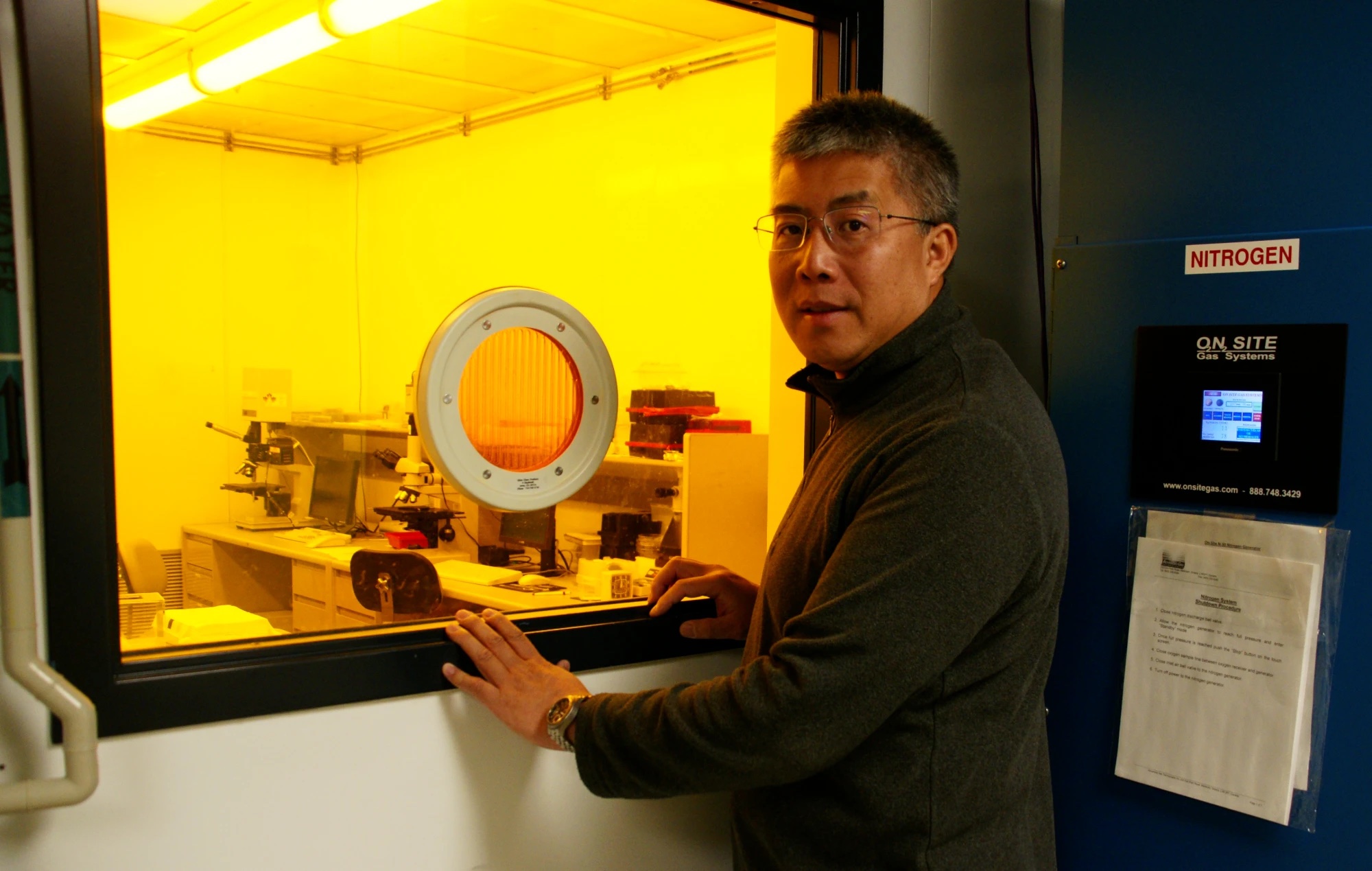
Professor Wai Tung Ng at the Toronto Nanofabrication Centre
Primus, our autonomous AI research system, has been set up to run research campaigns end to end inside the group's device design workflow: reviewing the literature, planning and launching hundreds of linked Synopsys Sentaurus TCAD simulations, analyzing the results, proposing the next design-of-experiment rounds, delivering designs and writing up findings. Researchers set direction, provide oversight and make key decisions.
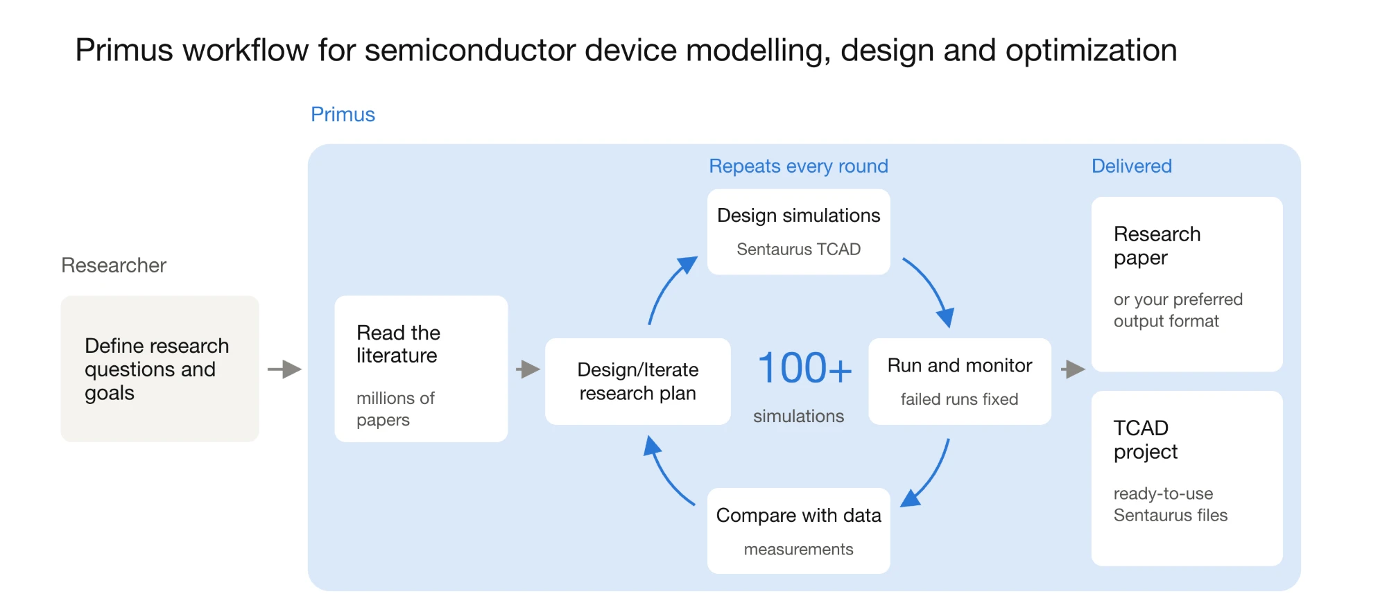
Figure 1: Primus workflow for power semiconductor device modelling, design and optimization.
Why power devices
Power semiconductors convert the electricity behind EV chargers, MRI machines, and every chip in a data center. Demand is outrunning supply: the IEA expects data center electricity use to roughly double by 2030, and Infineon has cited that the AI build-out is resulting in product shortages and price hikes. Better devices mean less wasted power and simpler, cheaper fabrication.
A key bottleneck is the range of possible designs to explore. A device study can have dozens of parameters, run across hundreds of coupled TCAD simulations. Researchers must painstakingly handcraft and track every combination they try. They use taste and judgment to pick the optimal paths that could reach a state-of-the-art design. That is the type of work Primus completely transforms.
Below are two early results from that work and observations on the impact Primus has had on the group’s research progress.
Early results
High-voltage MOSFET: Primus achieves lower resistance at the same voltage
A MOSFET is the switch at the heart of a power converter. When it is on, its resistance (on-resistance) wastes power as heat, so lower resistance means less energy lost on the chip. The difficulty is the trade-off between on-resistance and breakdown voltage. Adding more dopant to the device’s drift region lowers its resistance, but too much and the device can no longer withstand its rated voltage. Every watt a power switch doesn’t lose as heat reaches the GPU chip instead.
Primus took on that trade-off for a 200 V device. Primus autonomously reviewed state-of-the-art literature on high-voltage MOSFETs, planned a simulation campaign, ran simulations on TCAD by designing decks for the devices, analyzed all simulations, and proposed follow-up simulations to iterate and get to an optimum. Primus showed a strong understanding of the design and optimization dynamics applying an approach expected of a seasoned researcher in the field.
The final design, a 200 V silicon device with an optimized drift-region doping profile, reduced specific on-resistance down to 9.4 mΩ·cm². That is in line with the state-of-the-art performance the reference paper predicts.
With this confirmation of Primus’ capability, our research team will apply the proposed workflow to optimize other power semiconductor devices.
10 kV silicon carbide diode: Primus achieves one fewer manufacturing step while exceeding the published breakdown voltage
Next generation AI data centres are moving toward taking power straight from the medium-voltage grid, using solid-state transformers built on ultra-high-voltage diodes and switches. These diodes require optimized edge termination where the electric field crowds together. To prevent premature breakdown, engineers etch a staircase of steps into the device’s edge to spread out the electric field. Each step needs its own round of lithography and etching, which adds process complexity and cost.
Primus started from an ultra high voltage diode design published less than a year ago that used a four-step edge termination structure. Primus found a three-step design, with reduced fabrication steps, that exceeds the published breakdown voltage of 13.61 kV in simulation. In addition, Primus can document the reasoning behind each optimization decision. The design is also forgiving. Its breakdown voltage stays within 0.3 kV even if the etched steps are off by as much as 0.5 micrometres.
Primus then used the optimized dimensions in TCAD to generate the updated layout. This is the first design made end-to-end by an autonomous AI researcher. Once fabricated and verified, this AI generated design could provide exceptional performance with reduced fabrication overhead.
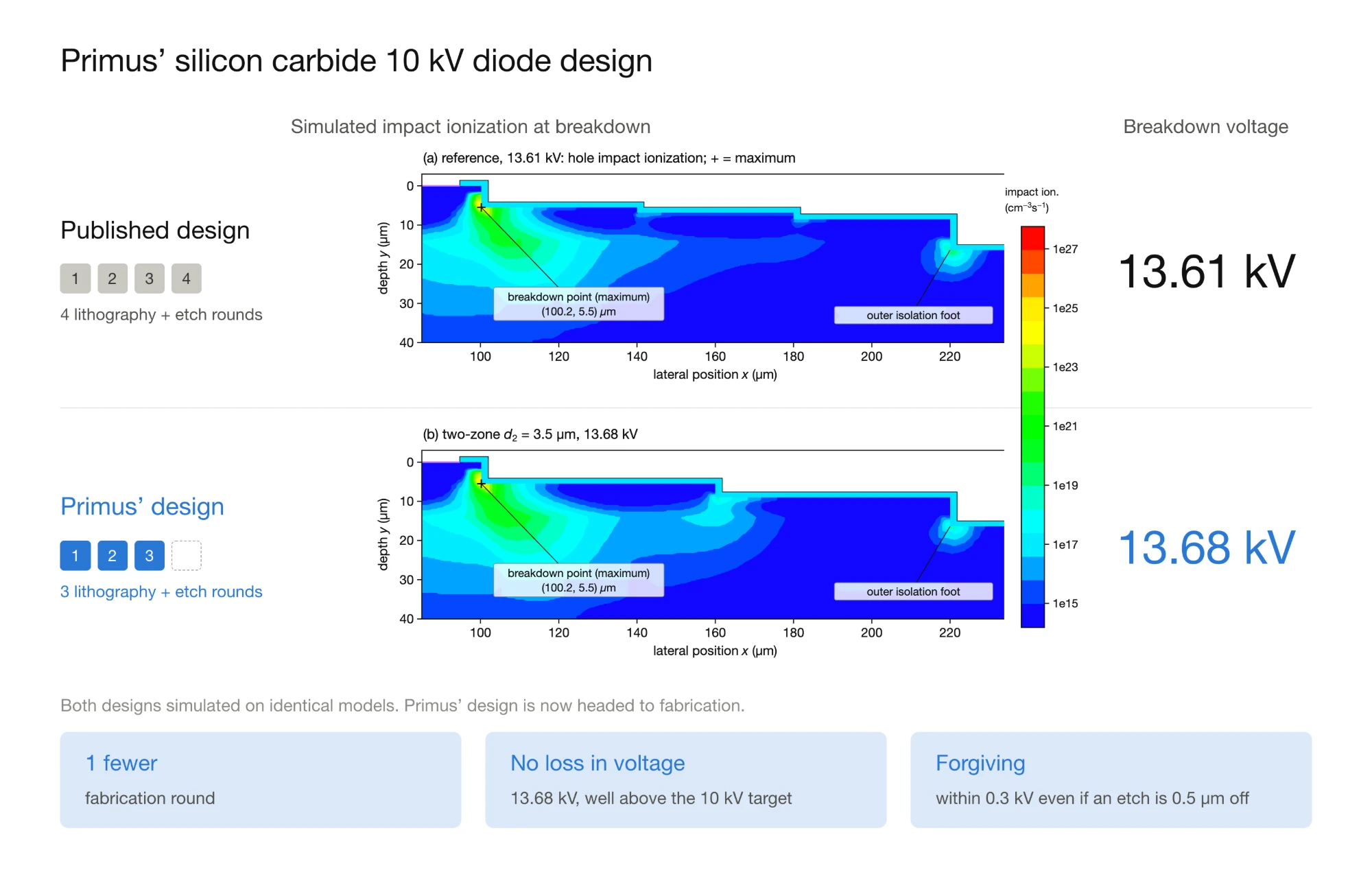
Figure 2: Primus’ silicon carbide 10 kV diode design
Time and effort
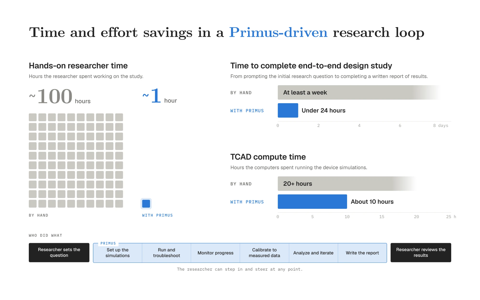
Figure 3: Time and effort savings in a Primus-driven research loop
In the case of Primus designing the 10 kV silicon carbide diode, it delivered a novel design while saving significant researcher time and effort across the experiment loop. Professor Ng’s group estimates this end-to-end study would have taken about 100 hours of hands-on work when performed without Primus. With Primus, the researcher spent about an hour setting the research question and reviewing the results. Primus ran simulations in parallel, handled deck setup, troubleshooting, monitoring, analysis, and report drafting completing the study within 24 hours.
“Primus is a transformative new approach to conducting semiconductor device research,” said Wai Tung Ng, Professor at The Edward S. Rogers Sr. Department of Electrical & Computer Engineering, University of Toronto and Director of the Toronto Nanofabrication Centre. “My team is now exploring a far wider range of device structures and pursuing ideas we previously didn’t have capacity for. We’ve also become less reliant on external experts like materials engineers to inform parameter tuning approaches. Primus is materially accelerating our design process. It’s leading to discoveries the manual approach may miss and reducing the steep learning curve in training the next generation of semiconductor device engineers. We are excited to partner with Transformer Lab to evolve this discipline.”
Work with us
As Professor Ng’s group continues to push Primus further into power device research, we are tackling hard open problems across fields such as chip design, quantum computing, mathematics, physics, biotech, quantitative finance and more.
If you’re interested in applying frontier autonomous AI research capability into your company or research group, contact us.